When Origami Meets Nuclear: The CEA Reinvents Neutron Detectors
The French Alternative Energies and Atomic Energy Commission (CEA) has developed a new type of neutron detector used to measure neutron activity in nuclear reactors. By leveraging additive manufacturing and specific shapes inspired by origami, the research organisation has created an innovative technology capable of withstanding the extreme conditions of these environments better than today’s equipment.
Nuclear fuel is not the only element found at the core of a reactor. It also contains a whole range of control and measurement devices used, for example, to anticipate component ageing or to measure neutron fluxes. This is precisely the purpose of neutron detectors, which therefore contribute to assessing the performance and safety of nuclear reactors. On 27 October 2025, the CEA announced that it had developed, in collaboration with the Magnetic Fusion Research Institute (IRFM), a new and innovative neutron detector capable of better resisting the extreme environments to which these components are exposed. This technological breakthrough has been patented, and the study’s findings are currently being published.
Protecting the neutron detector
Because of intense physico-chemical conditions (temperature, neutron fluxes, etc.), neutron detectors can age very quickly within the core. They therefore must be installed inside a robust capsule that protects them while still allowing them to perform their function. In this case, the neutron detector used by the CEA teams is a silicon carbide (SiC) diode, a semiconductor material capable of detecting a neutron by producing a signal. “Traditionally, sensors are mounted on complex and often fragile mechanical supports, poorly suited to extreme conditions,” explains the CEA. The scientists therefore devised two processes to address these weaknesses.
Additive manufacturing and origami
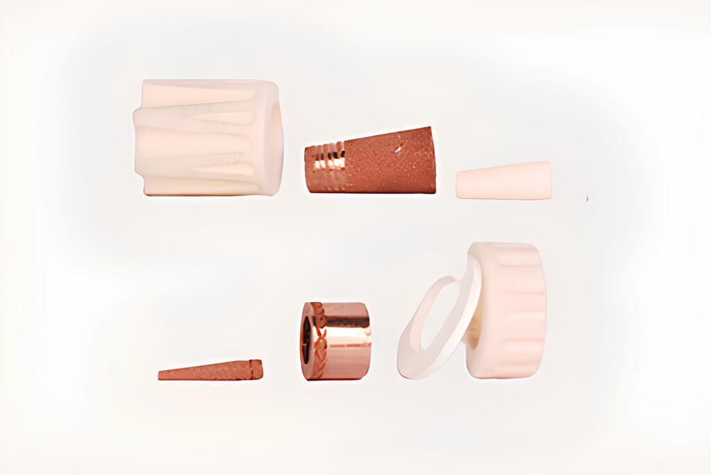
To create the protective piece, the researchers used additive manufacturing with two materials: an alumina-based material and a chromium-zirconium copper alloy (CuCrZr). Alumina is used for the insulating parts of the encapsulation. The alloy, on the other hand, offers excellent electrical and thermal conductivity as well as high mechanical strength. Additive manufacturing made it possible to overcome the constraints of traditional methods, particularly when producing complex geometries.
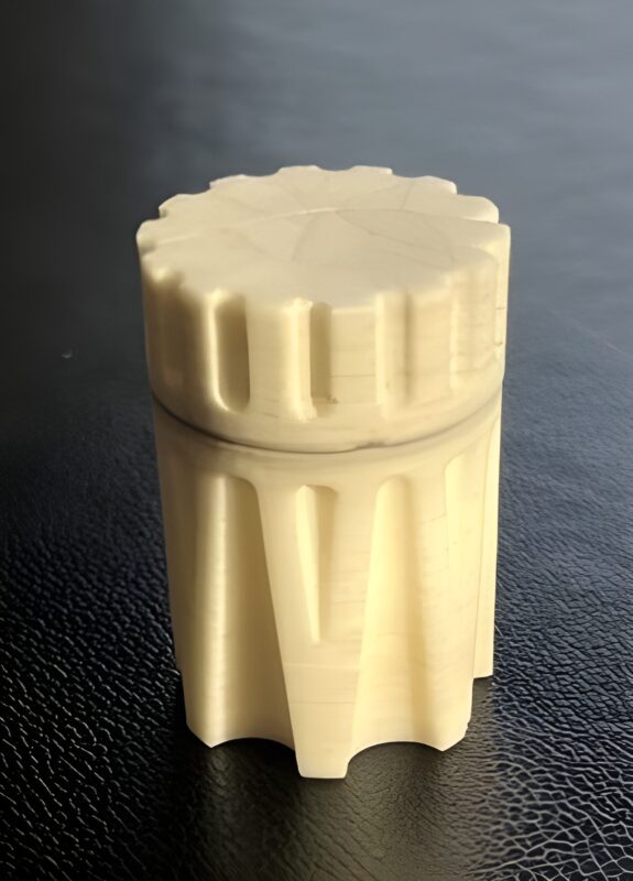
Prototype of a SiC neutron sensor encapsulation manufactured by additive processes – Source: CEA
The CuCrZr printed parts then had to be sealed together. The Spark Plasma Sintering (SPS) process was used for this purpose. It ensures both the mechanical integrity and electrical continuity of the assemblies. A powder with an origami-like structure was placed at the junction between the pieces. During the SPS cycle, the powder is heated, compressing the joint. This specific form helped “improve contact with the diode while refining the alumina walls to limit cracking at high temperature,” according to the CEA. “Optimisation work ultimately enabled the development of an ultra-fast SPS cycle that reduces material diffusion around the sensor, significantly lowers leakage currents and thus preserves the integrity and initial performance of the SiC sensor,” the commission adds.
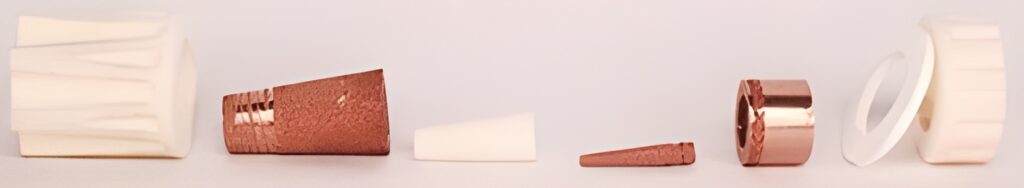
Insulating and conductive parts produced via additive manufacturing before assembly – Source: CEA
Validating the functions
Once the assembly was completed and sealed, the small component—15 mm in diameter and 25 mm high—was placed in a 14-MeV neutron generator. A final test confirmed that the neutron detector was able to carry out neutron measurements. In future, the new device could be used in the Jules Horowitz Reactor, in the ITER tokamak, or within the Laser Mégajoule.■